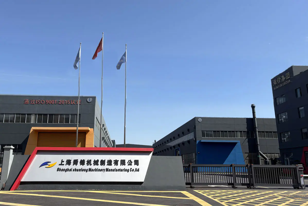




SUNFUN Group specializes in intelligent and sustainable industrial development. Driving quality advancement in manufacturing across China and the globe through technological innovation, we are committed to creating green value for a better human life.
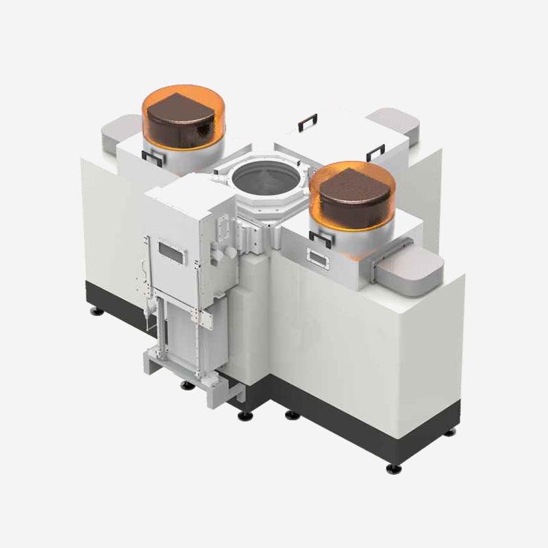
As China Wholesale HCALD Series Atomic Layer Deposition (ALD Coating) Equipment Factory and HCALD Series Atomic Layer Deposition (ALD Coating) Equipment Company, we have deep expertise in smart energy and smart manufacturing, consistently achieving breakthroughs in precision production. Our capabilities range from 0.001-mm precision machining to the manufacture of components weighing from 0.1 grams to 150 tons. We maintain energy consumption within 0.1% and implement fully intelligent process management—all supported by four decades of specialized experience!
Innovation is the foundation of the growth of our group. We have built an open and collaborative innovation ecosystem, partnering with governments, enterprises, universities, and institutions to enable cooperative innovation and shared value, injecting sustained momentum into the industry.
As an accredited technology enterprise with its own institute and talent academy, SUNFUN has completed more than ten national-level R&D tasks and undertaken major projects commissioned by agencies such as the NDRC, MOST, and MIIT. We offer HCALD Series Atomic Layer Deposition (ALD Coating) Equipment for sale.
อุปกรณ์และกระบวนการที่อธิบายไว้เกี่ยวข้องกับระบบการตกสะสมของชั้นอะตอมมิก (PEALD) ที่เสริมพลาสมาความจุสูง พร้อมระบบจัดการแผ่นเวเฟอร์อัตโนมัติและซอฟต์แวร์ควบคุม ALD เฉพาะทาง ช่วยให้การทำงานอัตโนมัติเต็มรูปแบบโดยใช้สารตั้งต้นต่ำ และความสม่ำเสมอและความสอดคล้องของฟิล์มที่ดีเยี่ยม ALD (Atomic Layer Deposition) เป็นเทคนิคการสะสมฟิล์มบางขั้นสูงที่ช่วยให้สามารถควบคุมการเจริญเติบโตของฟิล์มบนพื้นผิวของสารตั้งต้นในระดับอะตอมได้อย่างแม่นยำ ด้วยการสลับการสัมผัสกับสารตั้งต้นของไอสารเคมีที่แตกต่างกัน จะเกิดปฏิกิริยาพื้นผิวแบบจำกัดตัวเอง ส่งผลให้เกิดการสะสมตัวเป็นชั้นต่อชั้นเพื่อสร้างฟิล์มบาง ALD มีข้อได้เปรียบที่สำคัญเหนือเทคนิคการสะสมแบบดั้งเดิม โดยเฉพาะอย่างยิ่งในเรื่องความหนาของฟิล์มที่สม่ำเสมอและการครอบคลุมของส่วนประกอบที่มีรูปร่างซับซ้อน สามารถเคลือบได้สม่ำเสมอสูง แม้บนพื้นผิวที่มีโครงสร้างระดับไมโครหรือนาโน
มีการใช้กันอย่างแพร่หลายในเลนส์สายตา, Micro/MiniLED, อุปกรณ์ไฟฟ้า, OLED, MEMS, บรรจุภัณฑ์ขั้นสูง ฯลฯ
ใบสมัคร
ออปติคอล: ฟิล์มป้องกันแสงสะท้อน (ไม่มีแสงจ้าหรือแสงจ้า), ฟิล์มสะท้อนแสงสูง (T < 0.1%), ชั้นป้องกันเลนส์, อุปกรณ์ตะแกรง/ การเคลือบพื้นผิวโค้ง
เซมิคอนดักเตอร์: ชั้นทู่ชิป, ชั้นกั้น, ชั้นสื่อกระแสไฟฟ้า, ชั้นอิเล็กทริก ฯลฯ
ไฟฟ้าโซลาร์เซลล์: ชั้นทู่, ชั้นสื่อกระแสไฟฟ้าโปร่งใส, ชั้นกั้นไอน้ำ, ชั้นการขนส่งอิเล็กตรอน, ชั้นการขนส่งหลุม ฯลฯ
MEMS/เซ็นเซอร์: ชั้นฉนวน, ชั้นกั้นการแพร่กระจาย, ชั้นกั้นไอน้ำ, ชั้นที่ไม่ชอบน้ำ/ชอบน้ำ